2025. 9. 15. 18:00ㆍComputerScience/ProcessingInMemory
Pimba: A Processing-in-Memory Acceleration for Post-Transformer Large Language Model Serving
https://github.com/casys-kaist/pimba
GitHub - casys-kaist/pimba: Official code repository for "Pimba: A Processing-in-Memory Acceleration for Post-Transformer Large
Official code repository for "Pimba: A Processing-in-Memory Acceleration for Post-Transformer Large Language Model Serving [MICRO'25]" - casys-kaist/pimba
github.com
Abstract
- Transformers are the driving force behind today’s Large Language Models (LLMs), serving as the foundation for their performance and versatility. Yet, their compute and memory costs grow with sequence length, posing scalability challenges for long-context inferencing. In response, the algorithm community is exploring alternative architectures—such as state space models (SSMs) (e.g., Mamba- 2), linear attention, and recurrent neural networks (RNNs)—which we refer to as post-transformers. This shift presents a key challenge: building a serving system that efficiently supports both transformer and post-transformer LLMs within a unified framework.
- To address this challenge, we analyze the performance characteristics of transformer and post-transformer LLMs. Despite their algorithmic differences, both are fundamentally limited by memory bandwidth under batched inference—due to attention in transformers and state updates in post-transformers.
- Inspired by this finding, we propose Pimba, an accelerator solution that aims to address the memory bottleneck by jointly leveraging (1) Processing-in-Memory (PIM) paradigm and (2) LLM quantization. Further analyses suggest two additional insights: (1) state update operations, unlike attention, incur high hardware cost, making per-bank PIM acceleration inefficient, and (2) different low-precision arithmetic methods offer varying accuracy-area tradeoffs, while we identify Microsoft’s MX as the Pareto-optimal choice.
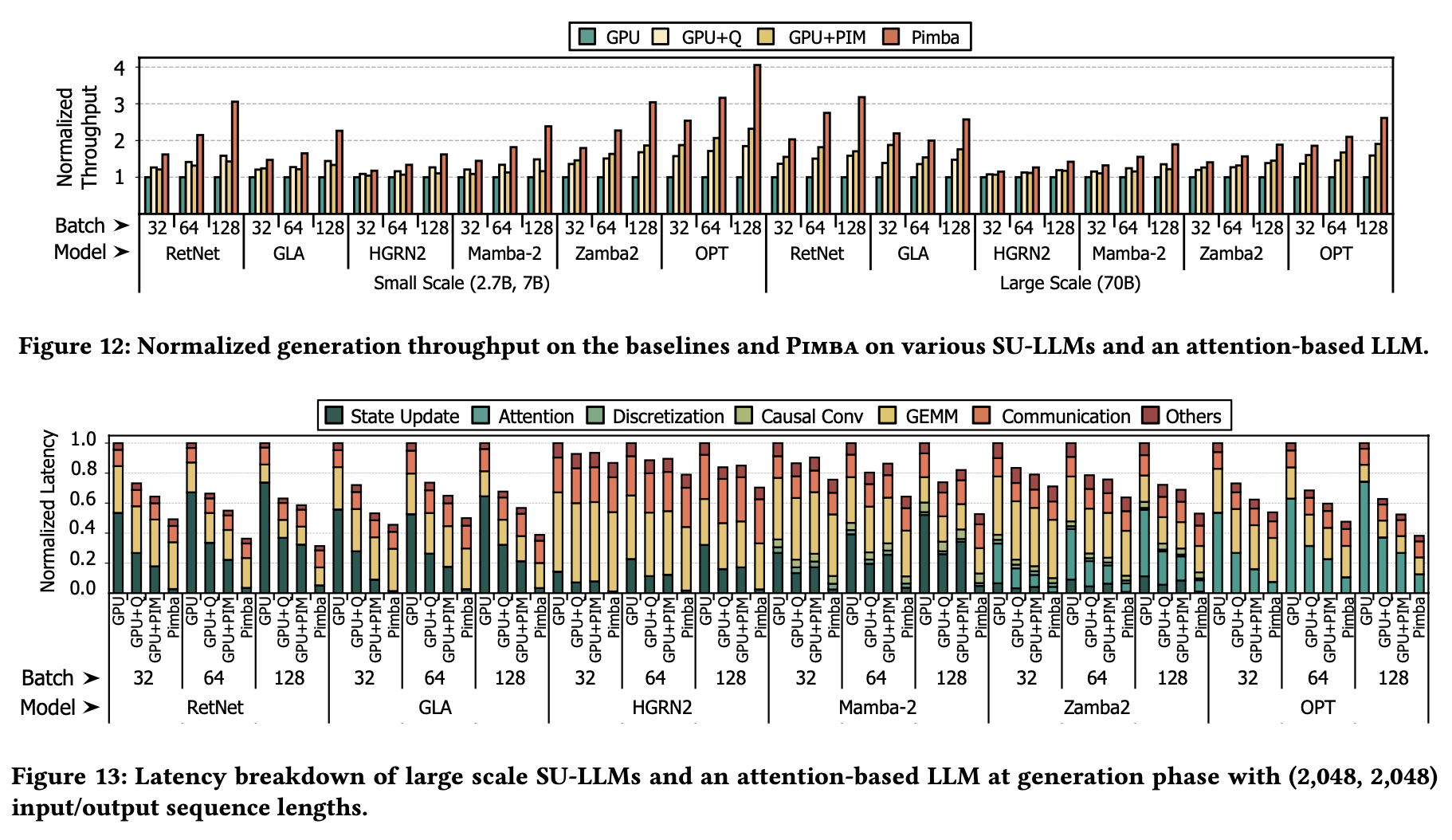
- Building on these insights, we design Pimba as an array of State-update Processing Units (SPUs), each shared between two banks to enable interleaved access to PIM. Each SPU includes a State-update Processing Engine (SPE) that comprises element-wise multipliers and adders using MX-based quantized arithmetic, enabling efficient execution of state update and attention operations. Our evaluation shows that, compared to LLM-optimized GPU and GPU+PIM systems, Pimba achieves up to 4.1×and 2.1×higher token generation throughput, respectively.

- Principle 1 : Maximizing hardware resource sharing for area efficiency: Existing LLM-targeted PIM acceleration methods [26, 27, 39, 53, 66] focus on supporting matrix-vector multiplication (i.e., GEMV) since attention operation is consisted of full of GEMVs.
- However, this approach is unsuitable for post-transformer algorithms since implementing the state update operation in hardware incurs significantly larger area costs due to the variety of primitives in state update operation, such as element-wise multiplication, element-wise addition, and vector dot products. Thus, in designing Pimba, we aim to exploit the hardware resource sharing for maximizing area efficiency.
- Principle 2 : Achieving both accuracy and area-efficiency from low-precision arithmetic: While quantizing the state in post-transformers can reduce computation cost and memory footprint, it also affects area efficiency. We also discovered that, due to the state “update” mechanism, conventional numerical formats cause severe accuracy degradation, rendering them impractical for post-transformers. We carefully explore the accuracy-area tradeoffs and observe that different low-precision arithmetic approaches exhibit different characteristics. We thoroughly perform an empirical study to understand the differences and aim to employ a Pareto-optimal (파레토 최적) quantization technique for our solution.

- State-update Processing Unit (SPU)
At the core of Pimba is the State-update Processing Unit (SPU), which includes a State-update Processing Element (SPE). Deploying an SPE for each bank would incur excessive area costs and reduce memory capacity, rendering this approach impractical under the stringent area constraints of PIM compute units. To address this, Pimba assigns one SPU to every two banks. The SPU alternates between reading from and writing to the row buffers of different banks, performing computations in an interleaved manner. This design sustains throughput while optimizing area efficiency. - SPE with MX-based quantized arithmetic
Empirical analysis suggests that among various quantization formats, MX8 [15] (requiring an average of 8 bits per value) emerges as a Pareto-optimal choice in the accuracy-efficiency tradeoff, while aligning seamlessly with memory address alignment requirements. This enables area-and power-efficient implementation of SPEs within the constraints of PIM. Consequently, we design custom MX8 vector multipliers and adders, significantly improving resource efficiency. - End-to-end Pimba system design
We construct the Pimba system by jointly leveraging Pimba accelerators with GPUs, offloading state update and attention operations to PIM, while delegating other tasks to GPUs. Pimba includes custom DRAM commands and command scheduling techniques to manage state pre-charging and subsequent generative computations. Our PIM accelerator and its interface use a system architecture similar to existing PIM-based LLM serving systems [27, 53, 54, 66], allowing Pimba to serve as a “drop-in replacement” in transformer-serving systems adapted to support post-transformer LLMs as well.
DRAM and Processing-in-Memory (PIM)
- DRAM architecture
DRAM is organized hierarchically, starting with channels, each divided into ranks, which are further subdivided into bank groups. Each bank group consists of multiple banks, with each bank storing data in a matrix format. - Accessing data from DRAM involves three critical steps: (1) Row Access: the sense amplifier of the bank activates the target row. (2) Column Access: the specific column within the activated row is selected, and the requested data is read out. (3) Data Transfer: the data is transmitted to the host via the data bus of the DRAM channel, where only one bank of the channel can transfer data at a time.
- PIM
Processing-in-Memory (PIM) is a realization of the Near-Data Processing (NDP) paradigm, which has branched into various research directions. Among these, industry-leading memory manufacturers focus on in-bank PIM technologies, where each DRAM bank is equipped with small compute logic to overcome the bandwidth constraints of the DRAM channel. These accelerators perform PIM operations during the first two steps of DRAM access, with computation handled by the in-bank logic instead of transferring data over the bus. - As DRAM comprises multiple banks, its internal bandwidth is significantly higher than the channel bandwidth, creating opportunities for PIM to leverage. Thus, PIM delivers substantial speedups for memory-bound tasks with low arithmetic intensity.
- Achieving both high throughput and area efficiency
We argue that even if the number of processing units in the per-bank pipelined design is halved, the same throughput can still be maintained, thereby achieving both high throughput and area efficiency. Even per-bank pipelined designs cannot fully utilize each processing unit because state updates require both read and write, and row buffers cannot perform both simultaneously. During writes, no input is supplied to the processing unit. With judicious dataflow Kim et al. design, two banks can share a single processing unit, allowing continuous input from both banks without throughput loss. We call this technique access interleaving and detail it in Section 5.2.
PIMBA Overview
- Overview
Building upon the aforementioned principles, we propose Pimba, a PIM-enabled system designed to accelerate state update and attention operations while minimizing PIM area overhead. We first focus on Pimba as a state update operation accelerator, while attention operation acceleration is detailed in Section 5.4. Figure 7 provides a high-level overview of Pimba system.
- Pimba system
Pimba handles user requests in two phases: prefill and generation. In the prefill phase, all operations, including state updates, run on the GPU, as they can be restructured into compute-intensive forms [14, 69]. In the generation phase, Pimba offloads the state update and attention operations to the PIM, while other operations remain on the GPU. For the PIM-executed operations, Pimba transfers operands to PIM registers, computes partial sums, and sends the results back to the GPU for accumulation. - To support heterogeneous execution, Pimba includes a software stack based on a prior work, HBM-PIM [39]. As in HBM-PIM [39], Pimba device driver first allocates physically contiguous memory blocks to facilitate efficient PIM operations. Custom GPU kernels are implemented for each Pimba operation to issue the necessary PIM commands and compute the addresses of the memory regions involved in the computations. To support this, the GPU programming model (e.g., CUDA) is extended with APIs to issue Pimba’s custom DRAM commands. (뒤에 5개 custom commands 구체적으로 나옴) When GPU kernels are compiled, these APIs are lowered to the corresponding custom DRAM commands. These kernels are then registered as custom operations within high-level frameworks such as PyTorch [5], allowing users to invoke Pimba functionality seamlessly through familiar APIs.
- PIM architecture
Pimba aims to accelerate state updates and attention while minimizing PIM area overhead. To achieve its objectives, Pimba introduces two key architectural innovations - 1) Pimba employs a novel State-update Processing Unit (SPU) that is shared between two memory banks (Section 5.2). Unlike traditional designs where a processing unit can only access one bank at a time for either read or write [39], Pimba’s pipelined design allows simultaneous reading from one bank and writing to the other. This overlapping of read and write operations across two banks enables Pimba to halve the number of processing units compared to a per-bank design, while maintaining the same throughput.
- 2) Within each SPU, Pimba integrates an MX-based State-update Processing Engine (SPE) to enable area-efficient and accuracy-preserving computations (Section 5.3). While prior works primarily focus on MX quantization for dot product operations [36], Pimba introduces a microarchitectural design specifically tailored for MX-based element- wise addition and multiplication.
- PIM banks with state data layout
We divide each state column along the 𝑑𝑖𝑚ℎ𝑒𝑎𝑑 dimension into sub-chunks based on the DRAM column size. Then, we group sub-chunks across the 𝑑𝑖𝑚𝑠𝑡𝑎𝑡𝑒 dimension to form a chunk that aligns with the DRAM row size, enabling efficient sequential access within each SPU. To further maximize operand reuse across chunks, we organize the chunks into chunk groups and assign each group to a DRAM bank. Chunks within the same group share the operands 𝑑𝑡, 𝑞𝑡, and 𝑘𝑡, and are placed in consecutive rows of the bank. - This arrangement enables the transfer of shared operands to Pimba once per chunk group, while only the corresponding 𝑣𝑡 vector is transferred per chunk, enhancing data reuse. Once assigned to banks, Pimba processes sub-chunks sequentially in a pipelined manner by reading consecutive columns within a DRAM row. In the 𝑖-th iteration (time unit during which Pimba processes each sub-chunk), Pimba utilizes the 𝑖-th sub-chunk, the shared 𝑑𝑡, 𝑞𝑡, 𝑘𝑡 vectors, and the 𝑖-th element of the 𝑣𝑡 vector in its computations.
Methodology

- Baselines
We evaluate Pimba against several baseline systems: an NVIDIA A100 GPU 80GB (GPU), the same GPU configuration but using int8 state quantization matching Pimba’s bitwidth (GPU+Q), and the GPU system with an HBM-PIM [39] (GPU+PIM). - Both Pimba and GPU+PIM systems adopt 40 HBM2E-based PIM memory modules operating at 1,512MHz, matching the bandwidth of the original A100 GPU memory. Given that SPU has a clock cycle of 𝑡𝐶𝐶𝐷 𝐿 (4 memory bus cycles), its frequency is 378MHz, which is consistent with prior work [39]. The HBM-PIM is designed using a time-multiplexed design that places a fp16 processing unit spanning two banks without the access interleaving technique of Pimba. This results in an area overhead comparable to that of Pimba PIM.
- For small scale models, all evaluated systems utilize a single GPU, as these models comfortably fit within one GPU’s memory capacity. For large scale models, all systems employ eight GPUs interconnected through a high-bandwidth network analogous to the NVIDIA DGX A100 system. We use NVLink3 as the interconnect for GPU-to-GPU communication, providing a bandwidth of 600GB/s, and the models are partitioned using tensor parallelism.
- Cycle-accurate simulator
We develop an in-house cycle-accurate simulator based on Ramulator2 [43] to evaluate the performance and energy efficiency of the PIM subsystem, incorporating existing DRAM timing constraints and refresh schemes. We model other system components including GPUs and NVLink by extending an open source simulator [53]. We refer to the activation and read energy of HBM from the previous work [51]. Detailed HBM configurations are presented in Table 1. - Cycle-accurate simulator - https://en.wikipedia.org/wiki/Computer_architecture_simulator (추가로 찾은 내용)
A cycle-accurate simulator is a computer program that simulates a microarchitecture on a cycle-by-cycle basis. In contrast an instruction set simulator simulates an instruction set architecture usually faster but not cycle-accurate to a specific implementation of this architecture; they are often used when emulating older hardware, where time precision is important for legacy reasons. - Often, a cycle-accurate simulator is used when designing new microprocessors – they can be tested, and benchmarked accurately (including running full operating system, or compilers) without actually building a physical chip, and easily change design many times to meet expected plan.
- Cycle-accurate simulators must ensure that all operations are executed in the proper virtual (or real if it is possible) time – branch prediction, cache misses, fetches, pipeline stalls, thread context switching, and many other subtle aspects of microprocessors.
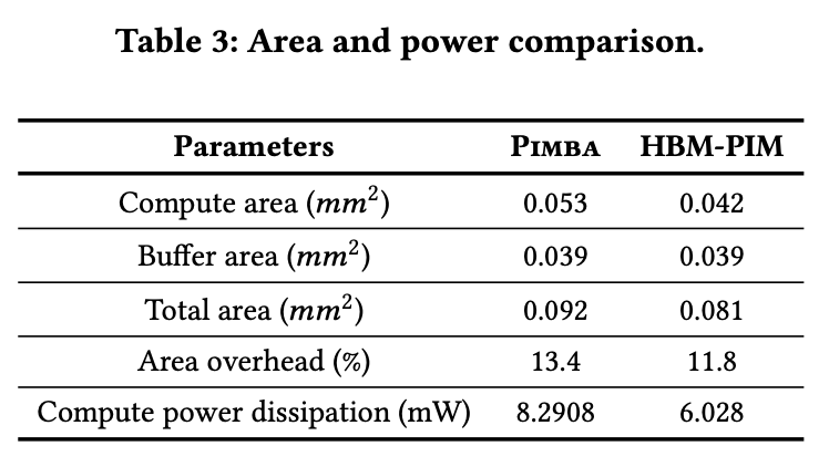
- Area and power
We synthesize Pimba accelerator using Synopsys Design Compiler with the FreePDK 45nm technology node [68], scaling area and power values to 10nm using the DeepScaleTool [64]. The same procedure is applied to the HBM-PIM, with components sourced from the Synopsys DesignWare libraries. Scaling follows methods from prior PIM works, considering that memory processes are 10×less dense than logic processes of the same feature size [53]. SRAM-based buffers are modeled using CACTI7 [7] at 22nm, then scaled to 10nm.
Conclusion
- This paper presents Pimba, a Processing-in-Memory (PIM) accelerator designed to efficiently serve both transformer and post-transformer LLMs under the increasing demands of long-context, high-throughput inference. Through detailed workload characterization, we identify that state update–a central operation in post-transformer models–shares similar memory bandwidth bottlenecks with attention in transformer-based models, motivating a unified acceleration approach.
- Pimba addresses these challenges by combining in-memory computation with quantized execution, co-designing its architecture around two key principles: (1) maximizing hardware resource sharing to reduce area cost, and (2) selecting Pareto-optimal quantization formats for efficient and accurate execution.
- Our evaluation shows that fine-grained access interleaving and MX-based state update engines enable Pimba to deliver significant improvements in throughput and area efficiency. These results suggest Pimba’s potential as a practical and generalizable solution for next-generation LLM serving infrastructure.
📌 참고자료
- https://github.com/CMU-SAFARI/ramulator2
- Ramulator 2.0 is a modern, modular, and extensible cycle-accurate DRAM simulator
GitHub - CMU-SAFARI/ramulator2: Ramulator 2.0 is a modern, modular, extensible, and fast cycle-accurate DRAM simulator. It provi
Ramulator 2.0 is a modern, modular, extensible, and fast cycle-accurate DRAM simulator. It provides support for agile implementation and evaluation of new memory system designs (e.g., new DRAM stan...
github.com
https://comsys-pim.tistory.com/15
Zsim + Ramulator (PIM simulator)
Zsim + Ramulaotor 는 Processing-in-Memory(PIM) 을 시뮬레이션 할 수 있는 프레임워워크로 향후 장기적으로 진행할 PIM 관련 연구의 Base line을 설정하기 위하여 정리했습니다. I. Introduction Zsim+Ramulator 은 Genera
comsys-pim.tistory.com
https://arxiv.org/abs/2403.00579
NeuPIMs: NPU-PIM Heterogeneous Acceleration for Batched LLM Inferencing
Modern transformer-based Large Language Models (LLMs) are constructed with a series of decoder blocks. Each block comprises three key components: (1) QKV generation, (2) multi-head attention, and (3) feed-forward networks. In batched processing, QKV genera
arxiv.org
https://ieeexplore.ieee.org/document/9499894
Hardware Architecture and Software Stack for PIM Based on Commercial DRAM Technology : Industrial Product
Emerging applications such as deep neural network demand high off-chip memory bandwidth. However, under stringent physical constraints of chip packages and system boards, it becomes very expensive to further increase the bandwidth of off-chip memory. Besid
ieeexplore.ieee.org
https://www.synopsys.com/implementation-and-signoff/rtl-synthesis-test/dc-ultra.html
Design Compiler: Timing, Area, Power, & Test Optimization | Synopsys
Design Compiler offers best-in-class RTL synthesis, enabling fast timing, small area, low power, and high test coverage within short design cycles.
www.synopsys.com